
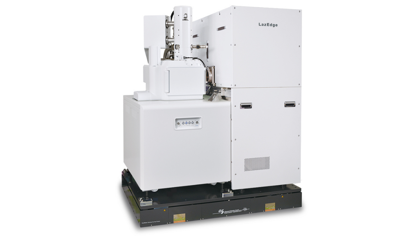
JEOL Ltd. (President & CEO: Izumi Oi) has developed the “LazEdge”, an SEM system equipped with a laser processing system, and began sales on May 25, 2026.
Cross-section preparation instruments, such as the focused ion beam system (FIB system), are widely used in science and technology fields across research institutes, universities, and industries. In recent years, demand has increased for a system that can process large areas at a high speed while achieving a high-quality processed surface. “LazEdge” is an instrument integrating JEOL’s SEM with the laser technology proprietary to Hamamatsu Photonics K.K., and enables laser processing inside the specimen chamber of the electron microscope.
This system enables high-quality cross-section specimens produced through high-speed, large-area processing to be transferred seamlessly to subsequent analyses, such as SEM observation, elemental analysis, and crystal orientation analysis, without exposure to the external environment. As a result, it meets a wide range of analytical needs, including metal specimen analysis, battery analysis requiring air-isolation, and semiconductor failure analysis requiring high-speed cross-sectioning.

[Main Features]
1. High-quality cross-sectioning inside the specimen chamber
By integrating a laser processing system into the SEM, LazEdge achieves high-quality cross-sectioning of large areas with reduced LIPSS structures at a high speed in the specimen chamber, through the use of a proprietary optical system that enables phase modulation of the laser beam spatially.
2. Stable and clean processing enabled by “LazEdge Shield”
The proprietary shielding technology “LazEdge Shield” minimises debris generated during processing from scattering and achieves clean processing without the contamination of detectors, columns, and specimen chamber walls. Moreover, the laser system can simultaneously focus on the specimen processing position and the laser irradiation position on the shield. This technology allows for the processing and cleaning of the shield (contamination prevention) at the same time. These technologies provide high-quality cross-sectioning while always maintaining stable power.
3. Seamless, high-throughput processing and observation
By installing a shield inside the SEM specimen chamber and performing the processing within the chamber, it is possible to carry out both processing and observation seamlessly and with high throughput. For example, in EBSD measurements, laser processing alone can produce a cross-section with sufficient quality for EBSD measurement. By automatically repeating the processing and measurement, 3D EBSD acquisition is also possible.
More related news:
proteanTecs and Gubo Partner on Unified Semiconductor Analytics
Rigaku Inaugurates XTRAIA MF-3400 to Measure Next-Generation Semiconductors
Agileo Automation to Expand A2ECF-SEMI Framework With SEMI EDA Standards