Avicena, one of the leaders in next-generation microLED interconnects, recently announced a major milestone at ECOC 2025 with a live demonstration of a fully operational microLED-based optical link operating at an industry-leading Tx power of 200 femtojoules per bit (fJ/bit) at <1E-12 raw bit error rate (i.e. no forward error correction). This achievement highlights the efficiency of Avicena’s scalable LightBundle platform for high-performance computing and AI data centers.
Using a high-sensitivity receiver, modified from a high-volume foundry camera sensor process, the demonstration link operates at dramatically reduced microLED drive currents. Since LEDs do not require the threshold current typical of lasers, they run fast even at low currents. In this live demonstration, the LED operates at about 0.25mA drive current and 4Gb/s and is paired with a hybrid-bonded camera sensor and discrete TIA.
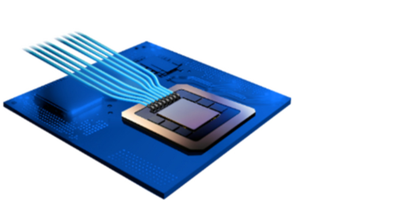
Scalable LightBundle Chiplet Platform for CPO Interconnects
Instead of serializing low-speed on-chip data (typically around 2 Gb/s per lane) to very high-speed optical lanes, LightBundle transmits raw parallel data directly, dramatically simplifying the architecture. This approach enables massive arrays of microLEDs to deliver unprecedented aggregate bandwidth at very low latency, low power consumption, and ease of integration with any silicon node. LightBundle chiplet transceivers are well-suited to various packaging architectures including co-packaged optics (CPO), on-board optics (OBO), pluggable optical modules, and wide memory interconnects.
“By leveraging a highly sensitive receiver, a minor modification to a high-volume camera process, and the unique properties of microLEDs, we can achieve unmatched energy efficiency in our LightBundle interconnects,” said Bardia Pezeshki, CTO of Avicena. “This breakthrough shows how microLED technology can replace legacy laser-based links with a simpler, more scalable, and far lower power solution.”
“The implications of this innovation extend beyond GPU-to-GPU connectivity,” said Marco Chisari, CEO of Avicena. “HBM memory interfaces are one of the next great frontiers for optical interconnects and ideally require wide buses with minimal latency. LightBundle’s ability to directly transmit low-speed parallel data at very low power and low latency, makes it ideally suited to breaking traditional memory bandwidth bottlenecks, and opening the door to new system architectures for next-generation AI and HPC platforms.”
This demonstration builds on Avicena’s ongoing work with hyperscale data center partners to enable scale-up GPU clusters spanning multiple racks and thousands of GPUs, and low power memory interfaces, to dramatically scale AI clusters and lower their power consumption.
Avicena at ECOC 2025:
In addition to showcasing its LightBundle interconnect technology at Booth C3517, Avicena will participate in the following events: Simon Richmond, VP of Operations, will be presenting at the Market Focus Session on Modules & Subsystems:
MicroLED-based Optical Interconnects for AI Data Centers: Advancing Scale-Up Networks Beyond Copper Interconnects.
Monday, September 29, 2025: 15:20 – 15:35


")