
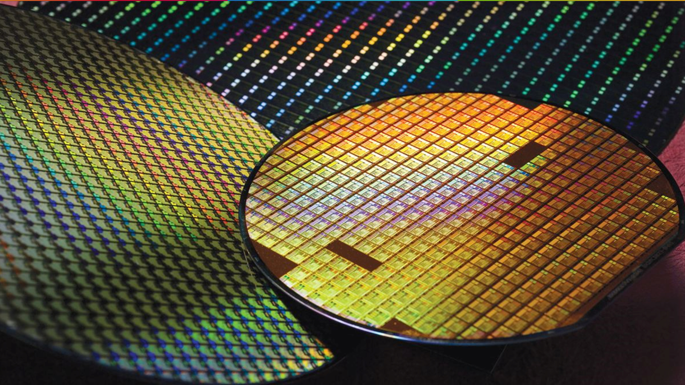
Cadence recently announced major advancements in chip design automation and IP, driven by its long-standing relationship with TSMC to develop advanced design infrastructure and accelerate time to market, for AI and HPC customer applications. Cadence and TSMC have collaborated closely across the spectrum from AI-driven EDA to 3D-ICs to IP and photonics, enabling the world’s most advanced semiconductors.
Cadence and TSMC have worked together on design infrastructure for advanced process nodes, including TSMC N3, N2 and A16, using CadenceInnovusImplementation System, Quantus Extraction Solution and Quantus Field Solver, Tempus Timing Solution and ECO Option, Pegasus Verification System, Liberate Characterization Portfolio, Voltus IC Power Integrity Solution, Genus Synthesis Solution, Virtuoso Studio and Spectre Simulation Platform. Cadence AI design flows for chip and 3D-IC are now available for TSMC’s advanced N3, N2 and A16 process technologies, as well as for new features in TSMC 3DFabric. Additionally, Cadence is collaborating with TSMC on EDA flow development for TSMC’s A14 process, with its first PDK to be released later this year. Further, several new Cadence IP are now silicon-proven and available for TSMC N3P.
“Cadence and TSMC remain committed to speeding up and improving the design process for advanced silicon for our customers,” said Chin-Chi Teng, senior vice president and general manager of the Digital and Signoff Group at Cadence. “We’re helping designers develop the next generation of AI and HPC by supporting TSMC’s leading technologies with AI features, IP and beyond.”
“TSMC, together with our Open Innovation Platform (OIP) partners like Cadence, is addressing some of the most intricate challenges in semiconductor development to drive higher performance and energy efficiency in AI systems,” said Aveek Sarkar, director of the Ecosystem and Alliance Management Division at TSMC. “Our enduring partnership continues to empower our mutual customers to accelerate their journey to silicon while driving the rapid proliferation of AI.”
AI-Driven Chip Design Solutions for TSMC Advanced Process Technologies
Cadence and TSMC have partnered on AI-driven design solutions for joint customers, enabling chip development with optimal power, performance and area (PPA) in TSMC N2. TSMC has enabled Cadence JedAI Solution, Cadence Cerebrus Intelligent Chip Explorer’s AI-driven implementation technology and productivity features powered by Innovus+ AI Assistant within Cadence’s digital full flow. Additionally, TSMC has validated new AI-driven features, such as automated design rule check (DRC) violation fixing assistance, enabling faster design closure and greater efficiency in the development of AI chips using TSMC N2.
Boosting Productivity for 3D-IC Designs
The Cadence 3D-IC solutions provide comprehensive support for TSMC’s advanced packaging and die stacking configurations offered by 3DFabric. The latest innovations include automation features for bump connections, physical implementation and analysis for multiple chiplets and smart alignment marker insertion. The AI-driven application of Cadence’s Clarity 3D Solver and Sigrity X Platform with Optimality Intelligent System Explorer enables and automates the 3Dblox-based system-level SI/PI analysis and optimization. Customers using TSMC Compact Universal Photonic Engine (TSMC-COUPE) multi-wavelength reference flow can utilize Virtuoso Studio with the Celsius Thermal Solver, along with productivity enhancements developed by TSMC and Cadence, including effective thermal simulation techniques for lowering the risk of declining electrical and photonic performance.
Leading-Edge IP for TSMC N3P
Cadence continues to drive innovation in AI and HPC by delivering silicon-proven, cutting-edge IP solutions on TSMC’s advanced processes, including N3P process technology, and helps customers build faster, more efficient and scalable systems. Cadence IP enables AI infrastructure by accommodating the memory and interconnect bandwidth capacity of next-generation AI LLMs, agentic AI and other compute-heavy workloads. New Cadence IP on TSMC N3P process technology includes the first HBM4 IP at N3P, high-speed memory interfaces like LPDDR6/5X at 14.4G and versatile DDR5 12.8G MRDIMM Gen2 IP that provide a wide range of options for customers as they address the memory-wall problem limiting AI compute systems. Cadence also leads in connectivity with PCI Express (PCIe) 7.0 IP—achieving a 128GT/s, 224G SerDes for AI infrastructure—and the first eUSB2V2 and Universal Chiplet Interconnect (UCIe) 32G IP that support emerging AI PC and chiplet ecosystems, demonstrating its commitment to driving energy-efficient, scalable solutions for future workloads.
Together, Cadence, TSMC and the OIP Ecosystem are empowering the AI supercycle by streamlining the customer journey from design to silicon and enabling customers to enhance design performance and energy efficiency.


")